OverviewThe following pages cover the step by step instructions on how to solder the Rev F PCB. (NOTE: The PCBs in the example pictures and videos are a prototype
version of the PCB and were mistakenly labelled Rev Ee)
Click the images to zoom in. All the construction example videos from these pages are also available on YouTube. Some good intro to soldering videos can be found at curiousinventor.com and also at sparkfun on YouTube (some of the videos may be upside down on this website).
1 - U1 VS1011 MP3 Decoder chip
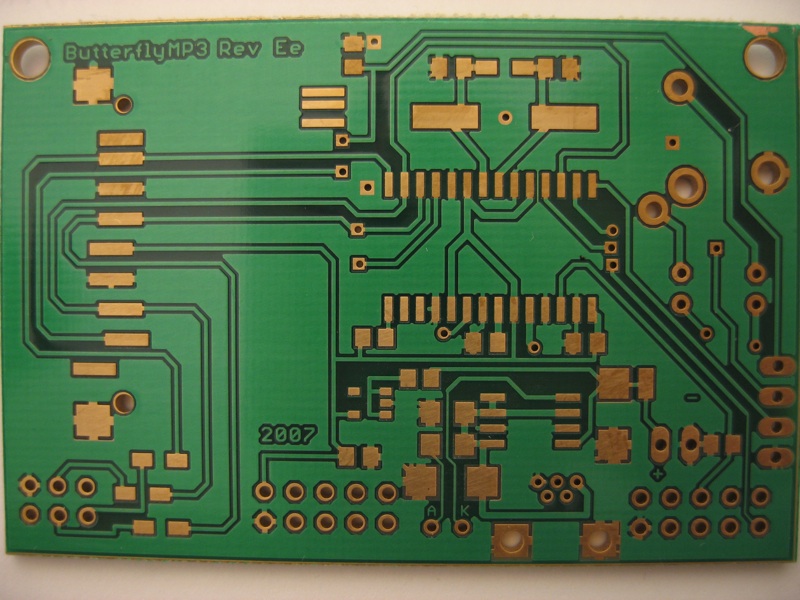
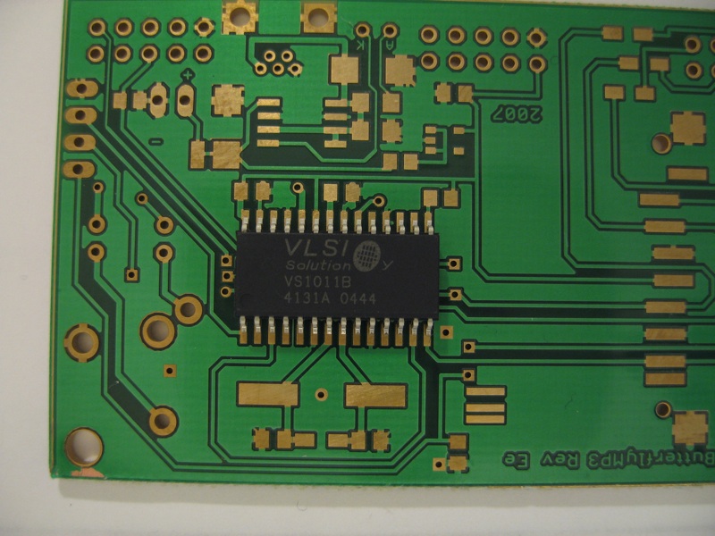
This is the first chip I solder to the board. As a general rule I like to start with the most difficult (or most expensive) ICs first. The reason is simply because with no other components on board I have the most flexibility in tackling the problem. In this case the chip is quite straightforward to solder and is probably not the most difficult on the PCB. It does however provide a good warm up for the slightly more difficult ones to follow. The first step is to check a new PCB for defects. Photo 1a shows the blank PCB before and soldering commences. The board should be checked for under or over etching. This is where the tracks may not been clearly separated (under etched) or where the tracks may have been removed entirely (over etched). This is uncommon with commercially fabricated boards but may occur if you have etched the boards yourself. Another problem to watch for is where there has been a board outline track etched in the copper layer as this can sometimes short signals near the edge of the board to the ground plane. Once the board has been visually inspected and looks fine we can start on our first component. I don't know how many PCBs I've designed but more often than not on a first run I get one of the footprints wrong or some minor mistake in the layout. So before we solder a component we should check it fits the PCB footprint on the board. Normally once I perfect a board a supplier will change a part and it will no longer fit. Photo 1b shows the VS1001 in position where we want to solder it. Make sure to note the position of pin 1 and the orientation of the chip. I talk about the VS1001 here but any of the VS10xx parts in the SOIC-28 package should work in this project so long as it has the compatibility mode to run like the original chipset. Below is a video showing how I normally attack this chip. There are many techniques for soldering this type of chip. One way is to put a layer of flux on the board, then place the component. Solder is then melted onto a large tip and dragged as a molten ball across the pins. This technique once mastered provides great results and is very fast. Extra flux (to that contained in the solder) is used as the solder is first melted on the iron tip and not the component pins/legs. This means the chemical cleaning flux from in the solder is consumed on the tip before the ball of molten solder is bought to the pins. The surface tension in the molten solder should mean that it forms small beads on each of the pins instead of simply bridging them as you might expect. As of yet I have not mastered this technique. Another technique uses "Solderwick" or de-soldering braid. You simply solder all the pins down without worrying about bridging the pins together. Once all the pins have been soldered you use the braid to remove any extra solder bridging the pins. The risks of this technique is that you can remove too much solder and leave some pins with an unreliable connection.The method can also cause pads to lift from the PCB if not done carefully. This is one of the quickest and easiest method but probably the riskiest. Sparkfun demonstrate this method this on YouTube. Solder-paste and reflow soldering is the industry standard manufacturing technique. All the pads are coated in solder paste using a laser cut metal screen to ensure that the paste only goes on the pads. Components are placed on on the PCB by a pick and place machine. The board is then heated in a precisely controlled oven. As the solder paste melts the components are soldered in place. This can be done at home simply using a frying pan or toaster oven (not to be re-used for cooking of course) with reasonable results. The paste screen can be omitted as the surface tension of the melted solder paste causes it to bead and resist bridging across closely placed pads. My method is the painful slow method using a small tip, small solder and pin by pin. Slow means more heat so you may end up overheating the chip which means you need to refrain from soldering consecutive pins. The following is the procedure I try to follow for most surface mount components including this one. It is suitable for a right-handed person holding the iron in the right hand, manipulating solder and components with the left.
Whatever the technique used the last step should always be to inspect the joins for cracks, bridging, icicles or any other defects and remedy as necessary. My results can be seen close up in Photo 1c above. The VS1001 is the heart of this design and is the reason it has a low component count, relatively simple PCB layout and requires very little power. The VS1001 MP3 decoder is also a digital to analogue converter and headphone preamplifier. Using other decoder systems such as STA013 or a software decoder would need more components and more power than this system. (It's basically plugging in an MP3 stream on one side and headphones in the other.)
|