OverviewThe following pages cover the step by step instructions on how to solder the Rev F PCB. (NOTE: The PCBs in the example pictures and videos are a prototype
version of the PCB and were mistakenly labeled Rev Ee)
Click the images to zoom in. All the construction example videos from these pages are also available on YouTube. Some good intro to soldering videos can be found at curiousinventor.com and also at sparkfun on YouTube (some of the videos may be upside down on this website).
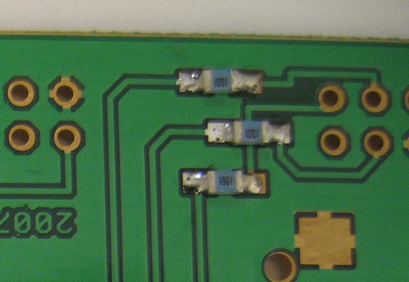
5 - R1-10 0805 SMD Resistors
The approach to these components is identical to that used for the 0805 SMD capacitors in the previous step. The resistors are slightly easier as they are normally marked with their values. The markings on the resistors follow the same system as through hole resistors with the exception that actual numbers are used in place of coloured bands. As you can see from the photos above you don't have to be neat and tidy to yield functional results. It does help trouble shooting later if all your resistors are aligned the same i.e. you can read the values without having rotate the board differently for each resistor. Also straight and centred resistors will produce more reliable connections in the long term but of course for a project like this is not essential. The technique I use is to add a small amount of solder to one of the pads for each resistor. The pad I choose is based on two factors. The main factor is the orientation of the PCB and which hand I hold the soldering iron in. For me as a right hander I use the right most pad. The second factor is if the pad is connected to a large track or plane on the PCB such as ground or the supply voltage. I would not use this pad for the first connection due to the extra heat required to make a reliable joint. Once half the pads have some solder I get the resistors ready. Normally I simply tip out all the resistors I will need on to an empty area on the PCB, trying to keep the different values together. Next I move all the resistors next to their destination with the tweezers, checking I have all the resistors needed and have them all in the correct place. Once I've checked my placement and values I then pick up the soldering iron again and begin soldering the resistors. Soldering the resistors is done in the same manor as the previous SMD components in the project. First heat the pad that already has solder on while holding the resistor to the left (in my right handed case) with the tweezers. When the solder is molten, gently but quickly slide the resistor into place. Now repeat this with the remaining resistors, heat and slide, heat and slide, until all the resistors are in place and soldered on one pad. If you are unhappy with the placement of any of the resistors simply reheat the pad, wait for the solder to melt and reposition the resistor. To complete the resistors run round the PCB soldering the remaining pads. Rotate the board as needed to keep the pad to the left (or right if you are left handed) of the soldering iron. For this step I find it most comfortable to solder with the unsoldered pad facing away from me. This means I can bring the soldering iron in from the right and introduce the solder on the left. It kind of forms a 'T' shape with the vertical stroke being the resistor and the left and right halves of the horizontal stroke being the solder and soldering iron. Although I don't follow the above mentioned procedure word for word in the video below it should give you a pretty good feel for how quick easy it is to solder these resistors. What do all these resistors do?R1 is used to load the crystal. This is part of the clock circuitry which provides a 12.288 Mhz clock to the decoder chip. R2 is used to pull down the MMC_CS line. This is used to detect the presence of the MC card without using the physical detect switch. To detect the MMC the MMC_CS line is held high for a moment and then switched to a high impedance input. After a short while (18 micro seconds) the value is read. If the line is still high then the MMC card is present. The MMC has an internal pullup resistance that holds the voltage high when the card is present. When the card is absent the 1 mega-ohm pull down resistor discharges the capacitance on the AVR input and allows the voltage to decay and after a short time produce a logic low on the line. While this method works well with most cards I have discovered the odd one or two for which this method fails. Software detection can be used in this case. Software detection is not used for all cards as it is slower and results in larger code size (albeit not much larger) R3 is necessary to hold the TEST0 line at the DVDD voltage (2.8V in this design). This is to keep the device out of test mode and because we are instructed to do this in the v1001 datasheet. R4,R5,R6 are placed in the SPI bus lines in between the add on board and the Butterfly. This is to avoid line contention if an external ISP programmer is connected to the Butterfly MP3 system. If the MP3 decoder or MMC card try to drive the SPI lines while the Butterfly board is being programmed the ISP programmer will overide any such interference. R7 will pull the VIN, SLEV, SELI, EN lines on the MAX1811 low when the usb power has been removed and C4 has discharged. I do not know why I did this. It appears at first glance that this resistor could be omitted. I probably misread the datasheet. R8 is the current limit for the battery charging LED. This limits the current to around 10mA. It was calculated as follows 5V (vIN) - 1.6V (vF red LED) = 3.4V, 3.4V/470R=7.23mA R9 is a pull down for the decoder reset line. This resistor forces the decoder to reset when the AVR Butterfly is reset or if the reset line is not driven by the AVR. This happens when the bootloader firmware is running. While the system is being programmed via the bootloader or simply in low power bootloader mode, R9 holds the decoder in reset. This stops any spurious signals from being emitted from the decoder and into the headphones. R10 is a one ohm resistor in series with the battery and the voltage regulator. This is used to monitor the current consumption of the circuit. For every mili-ampere drawn by the circuit the voltage drops by one mili-volt as per ohms law. The currents drawn by the circuit are low enough so that the wasted energy and dropped voltage are not enough to effect normal operation of the system. The voltage can be monitored on a scope and the effectiveness of sleep modes and total power usage can be evaluated.
|