|
|
Hardware Overview
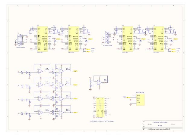
The schematic for the circuit is shown in Figure 1. The circuit is based around a number of RS232 line drivers and receivers (75C3243 from Texas Instruments); two of these are used on each input and have crossed wiring. When the system starts up it has all the transceivers disabled. The firmware then looks at the voltages on signal pins of the connectors and enables the appropriate transceivers.
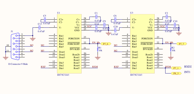
Transceivers / Line DriversTwo transceivers were used for each RS232 connection. Texas Instruments 75c3243 ICs were used as they were parts that were available to me at the time. In a future design I would consider using a dual or even quad transceiver chip such as the 64c232343 to lower component count. This system was not designed to be the cheapest solution but to be simple and straightforward to construct. The drivers were chosen simply because they were in stock on my workbench, in building a similar system any driver with a high impedance or shutdown mode would be suitable. In operation, an individual select line enables each chip. At most only one chip is ever active per channel at one time to avoid driver contention issues. The chips are operated in three modes. The first is high impedance mode, with both chips disabled. This state is used to examine the voltages present on the communications line with no excitation from the onboard drivers. With the first chip selected the channel is in normal mode. In this mode the pins of the DB9 are connected in standard configuration with pin two corresponding to the RXD (input) signal and pin three as TXD (output). In this configuration, the second chip is disabled. Lastly, in crossover mode the second chip is selected and the first is disabled. The second transceiver is wired with opposite connections to the DB9. This will have correct connections for a crossover/null modem cable. To keep the circuitry simple, only TXD and RXD signals were used. Flow control signals such as CTS, RTS and DTD could have been added but weren't used due to time constraints with the competition. This set up is repeated for each channel.
The TTL logic side of the two transceivers are connected in parallel and then are cross-wired and connected between channels. This ensures that the two channels have a correct connection. TXD from channel 1 (DB9M) is connected to RXD on channel 2 (DB9F). As a result of this there are only two TTL signals on the schematic RXF and RXM. These signals are connected to RXD1 (P6_2) and RXD2 (P7_1) respectively on the SKP demo board. This allows us to monitor the communications on each port individually. This crossover of the transceivers on the TTL logic side allows the system to function as an automatic null modem cable with minimal overhead on the micro-controller system. All the micro has to do is simply enable the appropriate transceiver for each channel. To allow the measuring and analysis of raw serial data these signals are also connected to two of the external interrupt channels available, INT1 and INT2. This allows the system to accurately detect level transitions.
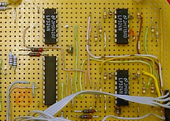
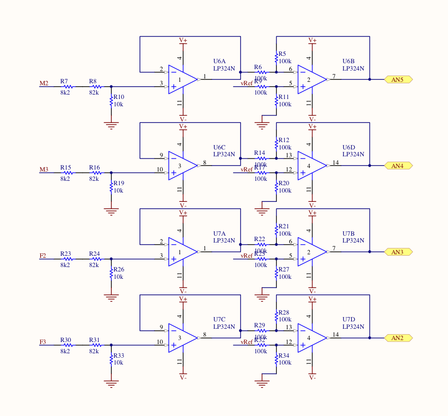
Voltage Scaling and SamplingIn the initial state, all transceivers are off and the inbuilt ADC measures the external voltage on the pins. A separate channel of ADC and op-amps, giving four channels in total, sample each pin voltage. The voltage on each signal pin is monitored though some basic op-amp circuitry. This is done to scale them from possible inputs of plus or minus 25 volts to the zero to five volts available to the micro-controller. The pin voltages are first scaled using resistors and then buffered using a voltage follower. The voltage is then inverted and shifted, centring it on the reference voltage. The reference voltage is half the micro-controller supply voltage (VCC) and is created by a simple resistive divider and a buffer. I initially considered multiplexing these signals through a single input stage but decided to go for the brute force approach for two reasons. Firstly op-amps are generally cheaper than analogue multiplexers. Secondly, with the SKP16C62P I had inputs to burn. In fact, four ADC channels is hardly a big ask of any modern micro-controller these days. A fifth RS232 driver was used simply to generate the plus and minus ten volts for the op-amp voltage rails. This was a MAX233ACPP. I used this as it was still sitting on the bench from another project and did the job nicely, needing no external parts. In a future design this would be eliminated and replaced by either using the existing drivers or a cheaper, more efficient, solution. Using this independent voltage generation allowed me to have all the 75C3243 ICs in shutdown mode until I had ascertained the correct connection polarity.
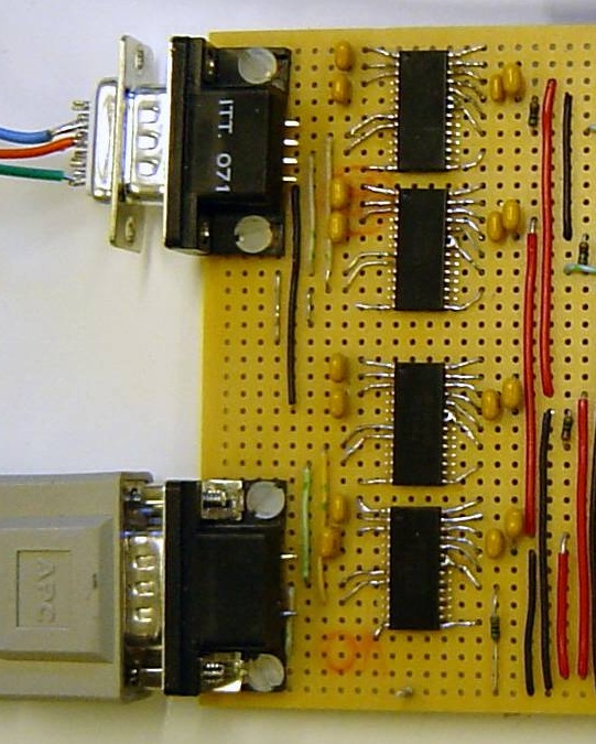
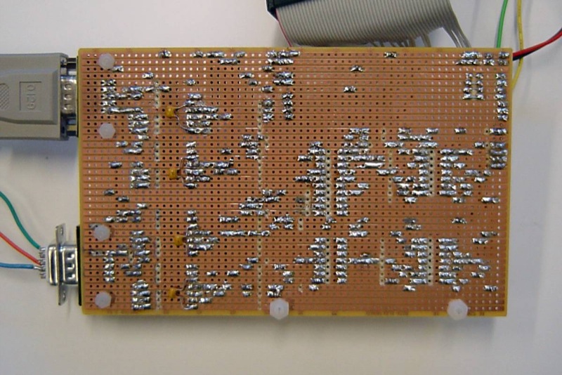
ConstructionFor the construction of this device I used strip-board to mount the components and the SKP16C62P. This was a good choice as the external circuitry is relatively simple consisting of mostly through-hole components. The transceiver chips I had available were all SMD 1.27 millimetre pitch small outline packages (SOIC). To mount these chips I simply ran un-insulated wire through holes in the strip board and then soldered to the pins on the chip sitting on the component side of the board. I was able to use this technique as a large number of the pins remained unused in the design. This has proved to be a pretty robust technique as all the chips are held firmly in place and have managed to withstand a fairly rough life being tossed about the workbench.
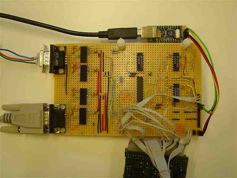
The demo board was mounted using standard PCB stand-offs over the sampling and scaling section. Photo 11 shows the component side of the board with the Renesas board folded out of view. The circuitry was connected to the demo board using an old 50-way IDC ribbon cable I had in a box of junk. This was great as it allows me to quickly and easily disconnect the demo board when I want to use it in other M16C projects and experiments. Any unused wires were simply tied back in a neat bundle out of the way. For those with a keen eye you'll notice that the hook up wire used is mostly single core from a salvaged length of "twisted-pair" telephone network. There are a few 0.1 micro-farad de-coupling capacitors not pictured on the underside of the board. |