About the Hardware
The latest revision board (Rev C) is available on the downloads page here. This is in Eagle format.
You can download EAGLE CAD from www.cadsoft.de.
Gerber files are also available.
Blank PCBs, Complete Kits and fully assembled shields are available from The Brokentoaster Shop
Schematics
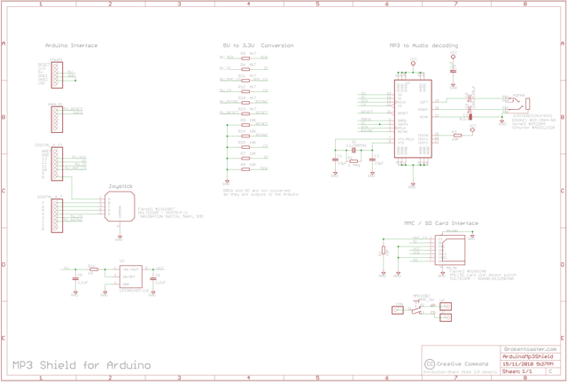 The current Arduino MP3 Rev C schematic.
The schematics and related info for the Arduino can be found
here.
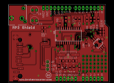
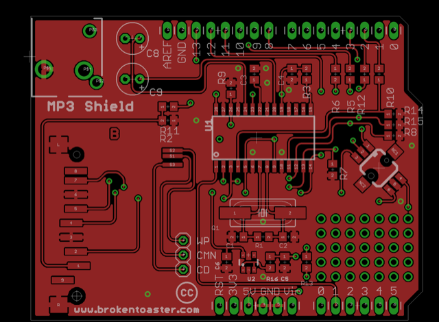
PCB Layout
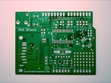
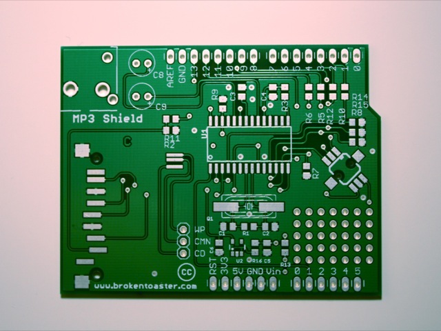
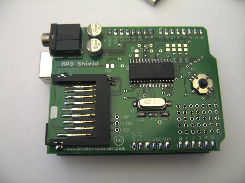
Top view of the PCB.
|

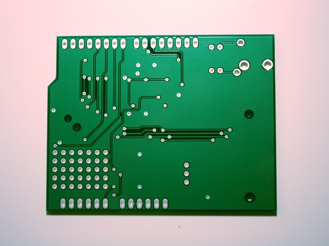
Bottom view of the PCB.
|
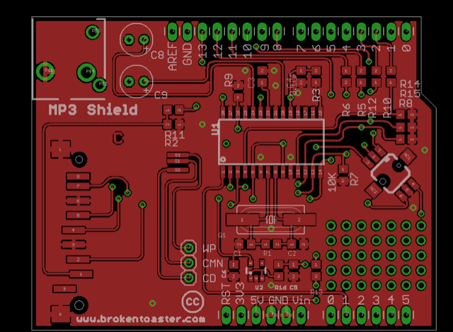
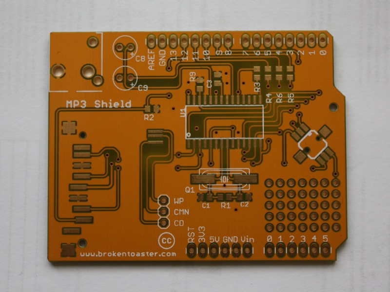
Top view of the PCB design (copper and silkscreen).
|
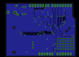
Bottom view of the PCB design (just copper).
|
PCB is FR4, double sided. 1oz (36μ) cu 1.6mm thick, solder resist, silkscreen topside
Bill of Materials
Current bill of materials
The following is the up to date bill of materials for the latest version of the PCB.
The parts are available from Farnell and Digikey with the exception of a few items.
If you cannot see the list below then it is also available here.
And where can I get those parts?
You can buy complete Kits from
my shop
The majority of the project parts are specified as standard parts from
Farnell
or Digikey.
Construction
You can build this project by simply soldering the parts to the PCB and plugging
it into your Arduino. You can use the next section on testing and trouble-shooting to test your work
Their are currently no specific build instructions for this project
published at this time. However much of the circuit is very similar to the
AVR Butterfly MP3 project
due to this project being a direct descendant of it. Until specific instructions are published
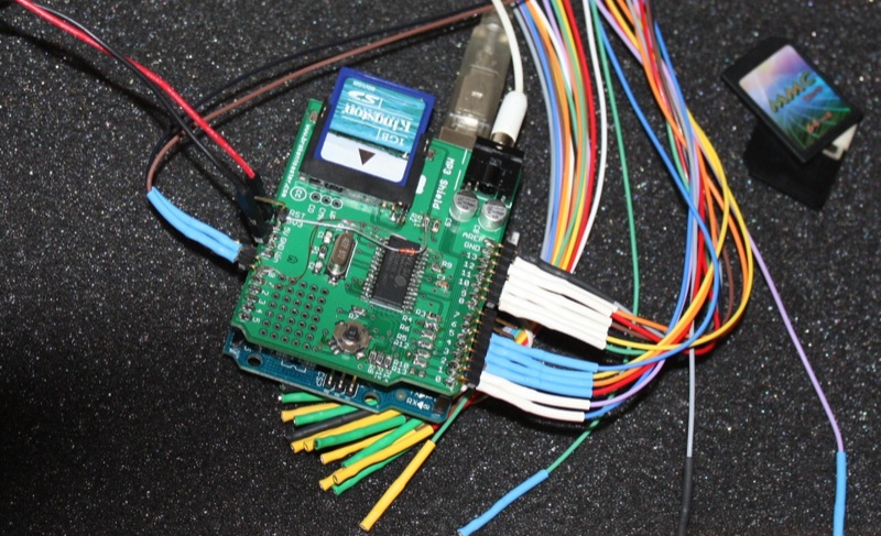
you can use the construction videos found
here and the photos to guide you.
Any questions are welcome in the Sourceforge forums
Testing and Trouble-shooting
| Pin name and description |
Signal
|
| |
Arduino Digital 0 - RX
5V asynchronous serial from the USB virtual com port to the Arduino.
|
|
| |
Arduino Digital 1 - TX
5V Asynchronous Serial communications from the arduino to the usb virtual serial port.
This is not used by the shield PCB itself but the demo software uses this to
transmit information
|
|
| |
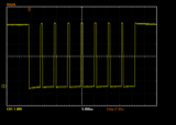
Arduino Digital 2 - 5V_BSYNC
This line is the 5V BSYNC signal from the arduino to the V1011 decoder. This is
used to synchronise the MP3 stream data when it is transmitted to the chip on
the SPI bus. The signal is high during the first bit of a data byte. See "7.3.3
SDI in VS1001 Compatibility Mode" in the data sheet for further details.
In New mode devices this is no longer BSYNC but an active low data chip select signal.
|
|
| |
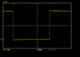
Arduino Digital 3 - 5V_CS
This signal is the chip select line for the VS1011E. It is later converted to a
3.3V compatible signal via a voltage divider of R12 and R15. When this line is low the
chip is accepting control data on the SPI lines.
|
|
| |
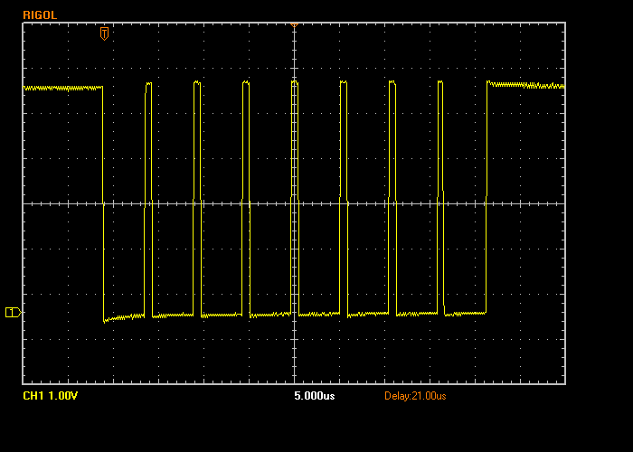
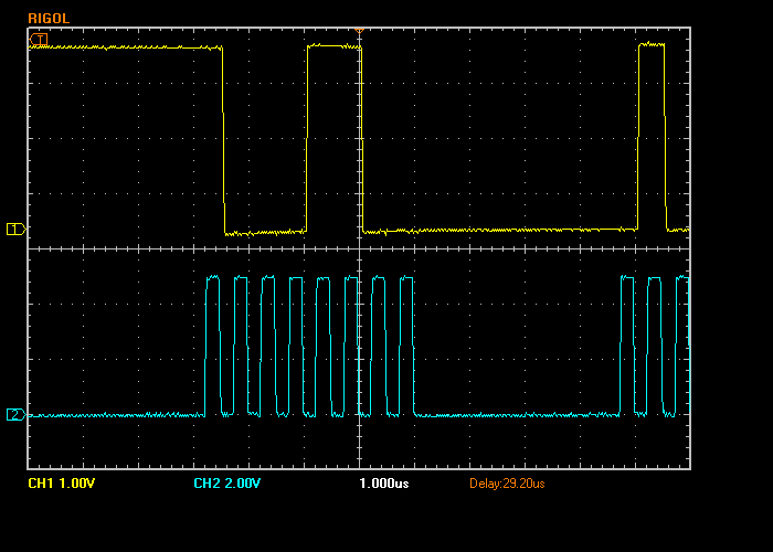
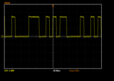
Arduino Digital 4, 5, 6, 7, 8 - Joystick
These groups of lines are connected to the joystick. They should have an internal
pull-up enabled on the arduino software. This means they normally sit at 5V when the
Joystick is in its normal state. When one of the directions of the joystick is
pushed this level will change to 0V. The software will de-bounce the signal by
looking for 20ms with no change in signal after an initial change in level. Although
de-bouncing is done in the software the signal shown looks very clean, perhaps
damped by stray onboard capacitances or probe capacitance.
|
|
| |
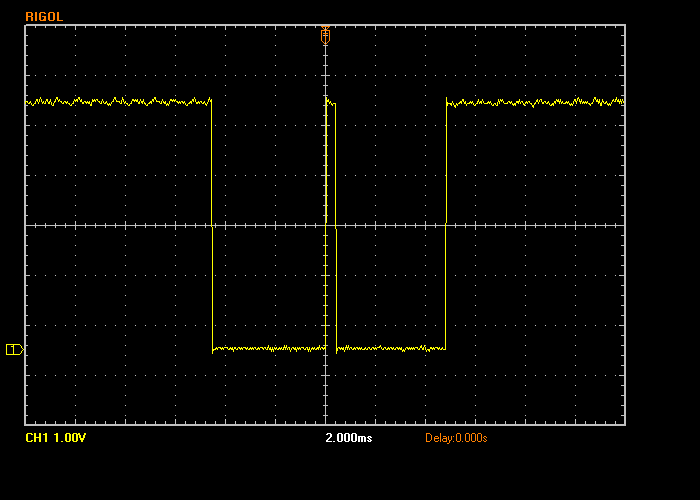
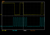
Arduino Digital 10 - 5V_MMC_CS
This signal is active low chip select for the MMC card. It is later converted to a
3.3V compatible signal via a voltage divider of R11 and R2. When this line is driven
low the MMC card will accept commands and output data on the SPI bus. This should
never be low at the same time as VS1011 chip select.
|
|
| |
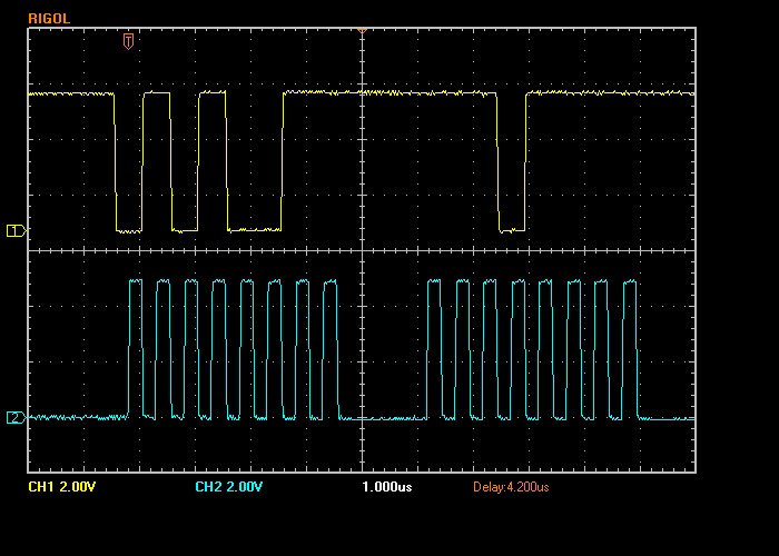
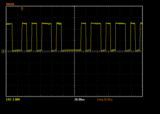
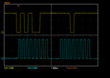
Arduino Digital 11 (5V SI) and 13 (5V SCK)
The SI signal is the SPI Serial In from the arduino to both the
MP3 decoder and the MMC/SD card. It is converted from 5V to 3v3 by resistors R6 and R7.
Line 13 is the 5V clock for the SPI Bus. This is converted to 3.3V by the voltage
divider of R5 and R8.
|
|
| |
Arduino Digital 12(3.3V SO) and 13 (5V SCK)
The SO signal is the SPI Serial Out from the MP3 decoder and
MMC/SD card to the arduino. It is not converted from 3.3V to 5V as 3.3V is
sufficient voltage to be registered as a high logic level by the arduino.
Line 13 is the 5V clock for the SPI Bus. This is converted to 3.3V by the voltage
divider of R5 and R8.
|
|
| |
Arduino Digital 14 (Analog 1) - 5V Reset
This is an active low reset line for the VS1011E. When this line is driven low
the VS1011e will be inactive and held in reset. The vs1011e will be in a low
power state with all it's IO pins disabled. This is normally 5V except at start
up or when resetting the the decoder chip. The 5V signal is converted to 3v3
volts for the vs1011E via the resistors R13 and R9.
|
|
| |
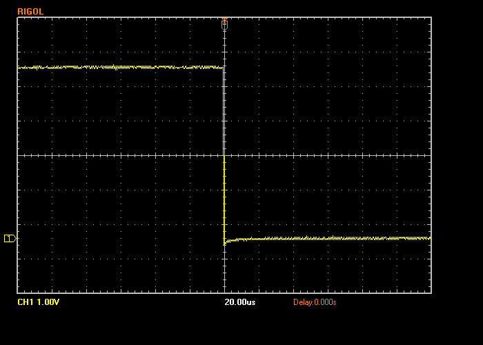
Arduino Digital 15 (Analog 2) - DREQ
This is a 3V3 logic output from the VS1011E connected to a 5V input of the Arduino.
This signal is high (3v3) when the VS1011 decoding engine can accept at least
another 32 bytes of data. It is used to signal the arduino software to stream
more data from the MMC to the chip.
|
|
| |
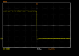
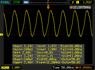
VS1011E Pin 7 (XT 1)
On this pin you should see the crystal oscillating at near 12.288MHz.
This will only happen if the chip is powered and enabled.
If you do not see this signal check the power (VS1011E pins 5, 9, 19, 28 and 23)
for 3.3V and check the reset line is high (VS1011E pin 26 has 3.3V at the chip).
If you find these voltages then check the soldering and values of the crystal,
loading resistor, and capacitors (Q1, R1, C1, and C2)
|
|
| |
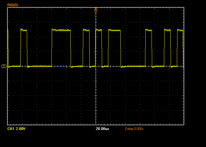
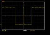
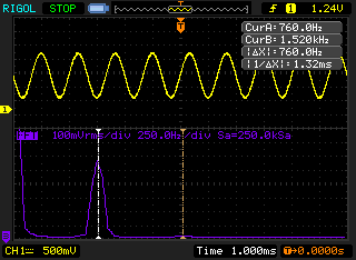
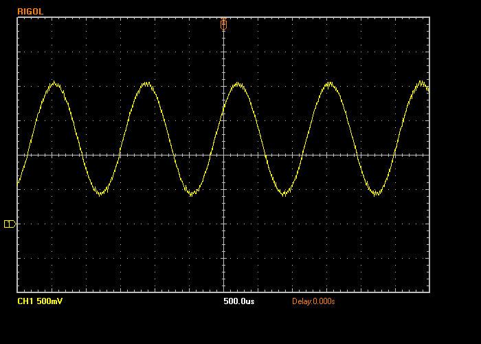
VS1011E Pin 20 (Right) and 24 (Left)
DC biased audio output on VS1011E pins 20 and 24. This shows the output while
running sine wave beep test.
The signal has a frequency of 760Hz. If this is not the frequency you see your
crystal may be oscillating at a different frequency or the registers on the chip
may not have been set up correctly. In particular check the setting of the clock
doubler in the software. The DC bias is removed from the signal by the two large
100μF capacitors C8 and C9.
|
|
|
Change History
|
The Rev_0 was designed to work with 3V arduinos only.
Arduino UART pins were used for some other function meaning communication with the
host PC was more difficult than it needed to been.
(The Yellow one and original Batch PCB)
|
Rev 0 PCB.
|
|
Rev 0 PCB.
|
|
|
The Rev_A was designed to work with 5V arduinos or 3v with a resistor mod.
Left the UART pins free. Didn't quite have enough oomph to drive mmc card and
decoder chip from the FTDI 3v3 regulator output (2 BatchPCB items were produced)
|

Rev A PCB.
|
|
|
The Rev_B board now includes National Semiconductor LP2891
ultra low dropout regulator. This supplies power to the MMC/SD card and the MP3
decoder from the 5V rail (never produced, Rev_0 was made due to my mistake)
|
Rev B PCB.
|
|
|
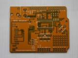
The Rev_C a minor couple of routing changes to the rev B no functional
differences. (produced, Green one)
|
Rev C PCB.
|
|